| Here's more about that nano-guitar... |
 The
new model! The
new model!
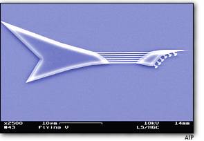
Oct. 28, 2003 Smallest guitar strummed at last: What does a 10-micron-long guitar sound like? Physics News Update reports that the Cornell nano-guitar, first built in 1997, has been played for the first time. Each silicon “string” of the nano-guitar is roughly 100 atoms wide, so you can’t exactly use a pick. Instead, a Cornell University research team used laser light to set the strings in motion, setting off a 40-megahertz twang. That’s 17 octaves higher than a normal guitar’s sound — put another way, a factor of 130,000 higher. “There is no practical microphone available for picking up the guitar sounds, but the reflected laser light could be computer-processed to provide an equivalent acoustic trace at a much lower frequency,” Physics News Update says. “The laser light could excite more than one string, creating megahertz ‘chords.’” The full story was to be told at the annual symposium of the American Vacuum Society, better known as the AVS. If the nano-guitar’s first notes are ridiculously high, a black hole’s tones are even more ridiculously lower, coming in at more than 50 octaves below middle C. At least that’s what Chandra researchers alleged in 2003.
|
The High and Low Notes of the Universe The Cornell nano-guitar, first built in 1997 but only now played for the first time, twangs at a frequency of 40 megahertz, some 17 octaves (or a factor of 130,000) higher than a normal guitar (see figure). Researchers at Cornell University used laser light to set the delicate silicon "strings" (actually slender planks of silicon) of the 10-micron-long guitar in motion. There is no practical microphone available for picking up the guitar sounds, but the reflected laser light could be computer processed to provide an equivalent acoustic trace at a much lower frequency. The laser light could excite more than one string, creating megahertz "chords." The playing of the nano-guitar will be described by Lidija Sekaric (now at IBM) at the AVS meeting (paper MM-WeM1; 914-945-1802). If the nano-guitar's natural tones are among the most high-pitched sounds in the universe, some of the lowest pitched are to be found in the vicinity of the black hole in the Perseus galaxy cluster. The Chandra x-ray telescope recently saw concentric circles in the inter-galactic gas cloud surrounding the cluster core; some astronomers interpret the ripples as being sound waves (with a frequency some 57 octaves below human hearing, and possibly "the deepest note ever detected from an object in the universe") caused by jets from the black hole shooting outwards into the nearby matter. (see Chandra press release) |

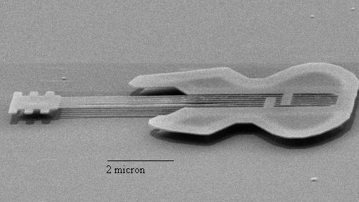
World's smallest silicon mechanical devices are made at CornellSmallest guitar, about the size of a human blood cell, illustrates new technology for nano-sized electromechanical devicesFOR RELEASE: July 22, 1997
The world's smallest guitar is 10 micrometers long -- about the size
of a single cell -- with six strings each about 50 nanometers, or 100 atoms,
wide. Made by Cornell University researchers from crystalline silicon,
it demonstrates a new technology for a new generation of electromechanical
devices. Photo by D. Carr and H. Craighead, Cornell. The above image (508 x 327 pixels) is the digital image created by the electron microscope, and is the highest-resolution version available. ITHACA, N.Y. -- The world's smallest guitar -- carved out of crystalline silicon and no larger than a single cell -- has been made at Cornell University to demonstrate a new technology that could have a variety of uses in fiber optics, displays, sensors and electronics. The "nanoguitar" - made for fun to illustrate the technology - is just one of several structures that Cornell researchers believe are the world's smallest silicon mechanical devices. Researchers made these devices at the Cornell Nanofabrication Facility, bringing microelectromechanical devices, or MEMS, to a new, even smaller scale -- the nano-sized world. "We have a new technology for building the smallest mechanical devices," said Harold G. Craighead, Cornell professor of applied and engineering physics who has the directed the work performed by his doctoral student, Dustin W. Carr. The guitar has six strings, each string about 50 nanometers wide, the width of about 100 atoms. If plucked -- by an atomic force microscope, for example -- the strings would resonate, but at inaudible frequencies. The entire structure is about 10 micrometers long, about the size of a single cell. A scanning electron microscope photo of the guitar (see above) won the award for best scanning electron micrograph at the 41st Electron, Ion and Photon Beam Technology and Nanofabrication Conference in Dana Point, Calif., in May. Carr and Craighead presented their research at the conference and submitted a paper to the Journal of Vacuum Science and Technology. While the guitar resulted in an award-winning electron micrograph, it is the other structures and devices that will be of real utility, Craighead says. Applications that require small-scale mechanical probes, high-speed response or measurement of very small forces can benefit from this technology. For example, mechanical force probes can be made much smaller than a single cell, and forces associated with single biological molecules could be measured. An efficient and relatively non-invasive method of measuring the
small motion of the mechanical structures is performed by using the interference
of laser light beams. The Cornell researchers have made a Fabry-Perot interferometer
using this technology. These interferometers use parallel mirrors, one
of which moves relative to the other. The motion is detected by variations
in the reflected light. The devices currently under study in Craighead's
laboratories are moved by electrical forces. These electrically driven
devices can be used to modulate the intensity of the reflected light.
In the near term, such nanostructures also can be used to modulate lasers for fiber optic communications. These researchers already have demonstrated the ability to make large amplitude modulation of light signals at high speeds. "We can make reflected light pulses at a rate of 12 million per second," Craighead said. Such a rate is faster than the bit rate of most ethernet connections. The structures also are extremely sensitive to very small forces. "We make these structures move and measure the motion by placing single electrons on the surface of the devices," Carr said. The key to the technology is electron-beam (or E-beam) lithography. E-beam lithography is a technique for creating extremely fine patterns (much smaller than can be seen by the naked eye) required by the modern electronics industry for integrated circuits. Derived from the early scanning-electron microscopes, the technique consists of scanning a beam of electrons across a surface covered with a thin film, called a resist. The electrons produce a chemical change in this resist, which allows the surface to be patterned. Most microelectromechanical devices are made by photolithography and chemical etching and have minimum feature sizes of slightly less than 1 micrometer. To build devices with dimensions of nanometers rather than micrometers requires a new fabrication approach. A nanometer is one-billionth of a meter. For comparison, the diameter of a human hair is about 200 micrometers, or 200,000 nanometers -- positively huge compared to these newest structures, where a wire is about 50 to 100 nanometers in diameter. "I know we can go smaller than this. The question is how small we can go and still have dependable and measurable mechanical properties. That is one of the things we would like to know," Craighead said. "We are nearing the technological limit where it gets harder to get smaller than this." Using high-voltage electron beam lithography at the Cornell Nanofabrication Facility, one of only two similar machines in this country, Carr and Craighead sculpted their structures out of single crystal silicon on oxide substrates. A resist is used to pattern the top silicon layer. The oxide that is underneath this layer can be selectively removed using a wet chemical etch. The result: free-standing structures in silicon crystal. "The nano-mechanical devices will also allow further exploration into important physical questions regarding motion and mechanical energy dissipation," the researchers wrote in their report. The Cornell Nanofabrication Facility (CNF) at Cornell University, is partially supported by the National Science Foundation. It is part of the National Nanofabrication Users Network, a partnership of nanotechnology centers across the nation. In addition, this research was funded partially by the U.S. Department of Defense and the Department of Education. |
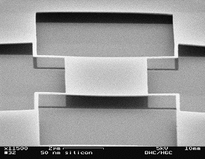 This 4-micrometer pad is suspended 400 nanometers above the underlying surface by "springs" that are 50 nanometers thick and about 200 nanometers wide. This structure has been tested and can be oscillated over the entire 400 nanometer range at rates of 7 million cycles per second. Photo by D. Carr, H. Craighead, Cornell. A higher-resolution, TIFF-format version of this image is available for download here. |
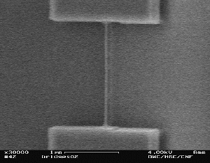 A 30-nanometer-wide wire is suspended across a 2-micrometer gap. The researchers believe this is the smallest known suspended structure that has been made in silicon. Photo by D. Carr, H. Craighead, Cornell. A higher-resolution, TIFF-format version of this image is available for download here. You know you need it for a desktop. |